FAQs
The current trend for the simplification, miniaturization and automation of the analytical systems have given the named Lab-On-a-Chip (LOC) or Micro Total Analysis Systems (µTAS).
A Lab-On-a-Chip (LOC) or Micro-Total Analysis System (µTAS) is a device that integrates one or several laboratory stages (sample pretreatment, mix, reactions, injection, separations, detection, etc...) on a very small (centimeters or millimeters) single chip. LOC devices provide new advantages in comparison with conventional analytical systems such as high speed, great versatility, high throughput, low cost, performance of parallel assays and negligible consumption of reagents/sample and waste generation [+].
Microfluidics, the manipulation of fluids in channels with dimensions of tens of micrometres, can be also considered a part of the Lab-on-a-Chip technology that has developed continuously and became a distinct new field.
A sensor (also called detector) is a device able to measure a physical quantity and converts it into a signal which can be read by an observer or by an electronic instrument.
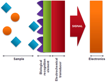
A biosensor is an analytical device for the detection of an analyte that combines a biological component with a physicochemical detector component [+].
Therefore, a biosensor consists of three main parts:
- A biological sensing element (biological material such as microorganisms, organelles, cell receptors, enzymes, antibodies, nucleic acids, etc).
- A transducer (electrochemical, optical, piezoelectric detectors, etc...) that transforms the signal resulting from the interaction of the analyte with the biological element into an easily measurable signal.
- Associated electronics or signal processors to display the results in a user-friendly way.
In case of using an electrochemical transducer, the biological recognition element can be immobilized in the electrode surface in order to get the biosensor.
Capillary electrophoresis is a powerful analytical technique used to separate ionic species with different migration times. It can be done due to the different charge to mass ratio of these species in a conductive liquid medium under the influence of an electric field [+].
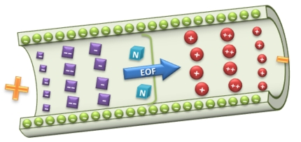
This separation technique is useful to separate small organic and inorganic ions as well as biomolecules such as proteins and nucleic acids (RNA and DNA).
Microfluidic electrophoresis chips can be considered an evolution through the miniaturization of the traditional capillary electrophoresis technique. Thus, these novel devices are the first stage to get a “true” Lab-on-a-Chip (LOC) in which would be integrated all the steps of an analytical process.
Microfluidics is an interdisciplinary field dealing with the behavior and control of extremely small volumes of fluids and the design of systems that use these small volumes [+].
Microfluidics, the manipulation of fluids in channels with dimensions of tens of micrometres, can be considered a part of the Lab-On-a-Chip (LOC) technology that has developed continuously and became a distinct new field.
Microchip electrophoresis (ME) is an emerging and highly promising method for fast analysis with minimum amount of analytes. Microchips electrophoresis can be enclosed as part of microfluidic and Lab-on-a-Chip devices.
Microfluidic electrophoresis chips have demonstrated to be a powerful tool for the development of novel analytical systems with multiple applications. Microfluidic electrophoresis chips enable the injection and separation of different compounds in a sample.
However, these devices require a miniaturized and sensitive detection system as well as an additional instrumentation in order to perform a full analysis. Among all detection methods, ectrochemical detection (ED) has proven to be very effective due to characteristics such as inherent miniaturization, sensitivity, low cost, portability and compatibility with microfabrication technologies. Nowadays, most of the electronic elements can be easily miniaturized. Nevertheless, the optical elements of different detection systems are not easily miniaturized without decreasing the performance. In this point, the electrochemical detection systems are easily miniaturized without decreasing the sensitivity and even improving the signal/noise ratio.
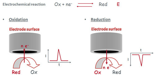
Electrochemical techniques are based on oxidation and reduction reactions (electron transfer reactions) which take place on an electrode surface [+].
Electrochemical detection systems show several important features such as selectivity, sensitivity, low cost, portability and compatibility with the microfabrication techniques.
These systems have been widely used in micro- and nanotechnology. Moreover, electrodes are a very useful tool in the construction of (bio)sensors.
Voltammetry groups a series of electrochemical methods based on the measurement of electric current applying different potential ramps. Depending on the potential ramps, there is several voltammetric techniques such as:
- Cyclic Voltammetry (CV)
- Linear Sweep Voltammetry (LSV)
- Differential Pulse Voltammetry (DPV)
- Normal Pulse Voltammetry (NPV)
- Square Wave Voltammetry (SWV)
- Alternating Current Voltammetry (ACV)
Voltammetric experiments are performed with a typical three-electrode sytem that consist of a working electrode (WE), a reference electrode (RE) and a auxiliary or counter electrode (AE / CE) [+].
Amperometry is an electrochemical technique based on monitoring the electric current generated in a redox process with time. It is a very useful detection method in flowing liquid systems (FIA, CE, HPLC...) and microfluidics
Different amperometric detection methods are available, such as single-potential amperometry (DC) or pulsed amperometric detection (PAD) [+].
Potentiometry is an electrochemical technique based on the measurement of the potential shift in a solution. Typically, the potential is measured between two electrodes; a reference electrode, with a constant potential, and an indicator electrode, whose potential changes with the composition of the solution. Therefore, the difference of potential between the two electrodes gives an assessment of the composition of the sample.
Potentiometry usually uses indicator electrodes made selectively sensitive to the ion of interest, also called ion-selective electrodes (ISE). The most common potentiometric electrode, by far is the glass-membrane electrode used in a pH meter [+].
A variant of potentiometry is chronopotentiometry which consists in using a constant current and measurement of potential as a function of time. In these experimets is used a typical three-electrode approach in order to a best control of the applied current into the cell without affecting to measured potential.
Electrochemical impedance spectroscopy (EIS) is a powerful non-destructive technique for characterizing a wide variety of electrochemical systems and for determining the contribution of electrode or electrolytic processes in these systems.
The principle of this technique is to apply an alternating signal of small amplitude (5 to 20 mV) to an electrode inserted into an electrolyte. The initial disturbance (applied) and the response of the electrode is compared by measuring the phase shift of the current and voltage components and by the measurements of their amplitudes. This can be done in the time domain or in the frequency domain, using a spectrum analyzer or frequency response analyzer (FRA), respectively.
Thus, some of the advantages of EIS include:
- The information content of EIS is much higher than DC techniques or single frequency measurements.
- EIS may be able to distinguish between two or more electrochemical reactions taking place.
- EIS can identify diffusion-limited reactions, e.g., diffusion through a passive film.
- EIS provides information on the capacitive behavior of the system.
- EIS can test components within an assembled device using the device’s own electrodes.
- EIS can provide information about the electron transfer rate of reaction.
Although, EIS data analysis can be very complex, it is a prowerfull tool with many promising applications including:
- Study corrosion of metals.
- Study adsorption and desorption to electrode surface
- Study the electrochemical synthesis of materials.
- Study the catalytic reaction kinetics.
- Label free detection sensors.
- Study the ions mobility in energy storage devices such as batteries and supercapacitors.
Photolithography is a process used in microfabrication to selectively remove parts of a thin-film (or the bulk of a substrate). It uses light to transfer a pattern from a photomask to a light-sensitive chemical on the substrate. These wafers are made on different materials: glass, silicon, quartz, polymers and also metals.
Photolithography (also known as "microlitography" or "nanolithography") works similarly to traditional lithography used in printing jobs. It also shares some fundamental principles with photography [+].
This technology is very useful in the manufacture of microfluidic devices as well as thin-film electrodes and microelectrodes.
Thin-film metal deposition is widely used in microfabrication processes. Different technologies such as physical (PVD) or chemical (CVD) vapor deposition can be used for thin-film metal deposition on several substrates (silicon, glass, polymers...).
PVD is characterized by a process in which the material goes from a condensed phase to a vapor phase and then back to a thin-film condensed phase. PVD processes include sputtering, evaporation, pulsed laser deposition, electron beam deposition, etc... [+].
In CVD, the wafer (substrate) is exposed to one or more volatile precursors, which react and/or decompose on the substrate surface to produce the desired deposit. Frequently, volatile by-products are also produced, which are removed by gas flow through the reaction chamber [+].
The combination of photolithographic processes, metal deposition and lift-off enables the fabrication of electrodes and microelectrodes with high precision and resolution for using in microfluidic devices and sensors.
Lift-off process in microstructuring technology is a method of creating structures (patterning) of a target material on the surface of a substrate (e.g. wafer) using a sacrificial material (e.g. photoresist). It is an additive technique as opposed to more traditional subtracting technique like etching. The scale of the structures can vary from the nanoscale up to the centimeter scale or further, but are typically of micrometric dimensions [+].
Etching is used in microfabrication to chemically remove layers from the surface of a wafer during manufacturing. Etching is a critically important process module, and every wafer undergoes many etching steps before it is complete. Different processes such as wet etching or dry etching can be used for removing layers from specific wafer materials [+].
Wet etching processes use liquid-phase ("wet") etchants. The wafer is immersed in a bath of etchant, which must be agitated to achieve good process control. The selection of the solution (etchant) employed for this process is critically important. For instance, buffered hydrofluoric acid (BHF) is used commonly to etch glass substrates or silicon oxide based substrates.
Dry etching refers to the removal of material by exposing the material to a bombardment of ions (usually a plasma of reactive gases such as fluorocarbons, oxygen, chlorine, boron trichloride; sometimes with addition of nitrogen, argon, helium and other gases) that dislodge portions of the material from the exposed surface [+]. A common type of dry etching is reactive-ion etching (RIE) and deep reactive-ion etching (DRIE).
Unlike with many (but not all) of the wet chemical etchants used in wet etching, the dry etching process typically etches directionally or anisotropically.
In microfabrication technologies, a bonding process involves the sealing of different open microestructures in order to get fully-closed devices. Different technologies can be used in this process such as thermal bonding, anodic bonding or adhesive bonding.
A thermal bonding process is used to bond two surfaces, usually the same material, by applying pressure and temperature close to glass transition temperature (Tg) of the material [+].
Anodic bonding is a wafer bonding process to seal glass to either silicon or metal without introducing an intermediate layer; it is commonly used to seal glass to silicon wafers in electronics and microfluidics. This bonding technique, also known as field assisted bonding or electrostatic sealing, is mostly used for connecting silicon/glass and metal/glass through electric fields [+].
Adhesive bonding (also referred to as gluing or glue bonding) describes a wafer bonding technique with applying an intermediate layer to connect substrates of different materials [+].
MicruX products' portfolio includes:
- Electrochemical sensors & platforms.
- Microfluidic devices & platforms.
- Portable analytical instrumentation.
- Other accesories for electrochemistry and microfluidics.
Users can browse throughtout our online catalogue in orde to find out more about our products and services.
MicruX is proficient in thin-film metal-based electrodes and microelectrodes manufactured with features up to 5 microns. Thin-film technologies enable the manufacture of different (micro)electrode design including microelectrode arrays (MEA), interdigitated electrodes (IDA / IDE) and interdigitated ring array electrodes (IDRA).
Moreover, thin-fim (micro)electrodes can be easly integrated with a microfluidic stage in order to get more versatile devices for multiple applications.
Electrochemical sensors are manufactured on a glass substrate. Currently, electrodes are available in metal gold or platinum with a thickness of 150 nm. A titanium layer (50 nm thickness) is used as adhesion layer between glass substrate and functional metal (gold or platinum).
Standard electrodes are provided with a insulation layer of SU-8 resin, in order to passivate the non-functional parts of the sensors, keeping open the electrochemical cell and electrical pads. Electrodes can be also provided without the insulating layer.
MicruX provides microfluidic chips (standard microchips electrophoresis and thin-layer microfluidic sensors) manufactured in hybrid material of SU8/Glass. Microfluidic channel structures are built in SU-8 resin on a glass substrate. The cover plate with inlets/outles is also manufactured in SU-8 resin.
Other materials can be studied under previous request.
Yes. Technologies available in MicruX enable the possibility of tailored devices to fulfill the requirements of customers. In this case, the price will be different to the standard devices. Anyway, we can elaborate a quotation without any compromise.
Customers have different options for purchasing MicruX' products:
- Purchase order submitted by e-mail or fax. Customers can contact directly to us by e-mail (sales@micruxfluidic.com) or phone (+34 984151019) in order to get a formal quotation for the products they are interested in. The quotation will be sent to them asap, usually, 24 - 48 hours. After that, they can submit their purchase order confirmation (indicating the quote number) by e-mail or fax.
- MicruX online store. Registered customers can browse throughout our webstore to add the products they are interested in to the online shopping cart. Thus, they can process directly the purchase and payment throughout our secure online store. A confirmation will be send to you by e-mail at the end of the purchase process. This is a very fast and effective way to process the purchase of MicruX' products.
Registered users (by creating a free account) can check the prices of each MicruX' products directly in the online webstore. Prices shown in the online store are EX-WORKS and they do not include taxes, fees nor shipping costs. Shipping costs and taxes are included at the end of the purchase process.
In this sense, creating an account in MicruX website has also other benefits like the posibility of follow your orders status and save your shipping and billing addresses for future orders.
- Mora-Garay Industrial Park · Building #6 · Juan de la Cierva, 2C, 33211 Gijón (Asturias), Spain
- Phone/Fax: (+34) 984 151 019
- Email: info@micruxfluidic.com
- Web: www.micruxfluidic.com
Contact
MICRUX® - All rights reserved - 2024